Switches
What a Solid-State Microwave Switch Is
No moving part, one mechanism, and three numbers that come out of it. This is the primer the rest of the switch section is built on.
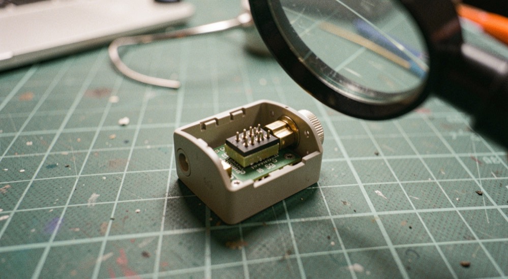
A solid-state microwave switch is a component that routes a microwave signal without a moving part. It opens or closes a path by driving a semiconductor junction between two states: low impedance, where the path conducts, and high impedance, where the path blocks. Above roughly 100 MHz the junction doing that work is, most often, a PIN diode. Port counts, placements and the three headline figures all follow from how that junction is wired and driven.
A junction that decides, not a contact that moves
The PIN diode takes its name from its middle layer: an intrinsic region sits between the p and n regions and stores charge carriers. Above a transit frequency, the stored carriers change the junction's behavior completely. It stops acting as a rectifier and acts as a resistance whose value the direct bias current sets. That is the basis of the whole part here: a control current varies an RF impedance, so the signal is switched without being detected. Forward biased, the diode presents a low series resistance and the path conducts. Reverse biased, or at zero bias, the junction presents a small capacitance and the path blocks. On and off are impedance states, chosen with DC power on the control line.
Series, shunt, or both?
Placement decides what the circuit is good at before any figure is printed. A series diode sits in the signal path: its forward resistance shapes the conducting path, its off-state capacitance limits how completely the path blocks. A shunt diode sits between the path and ground: biased on, it short-circuits the line and the signal is reflected; biased off, its capacitance still hangs across the path. Driving both together, shunt diodes biased in complement to the series ones, buys isolation neither element reaches alone, at the price of extra resistance in the on state. What the blocked port shows the source is a fourth choice, the one split in absorptive against reflective designs.
| Arrangement | What it fixes first | What it costs |
|---|---|---|
| Series element | The conducting path: forward resistance sets the loss | Blocking stays limited by the junction capacitance |
| Shunt element | The blocked path: an on-state diode short-circuits the line | Its off-state capacitance sits across the path |
| Series with shunt | Isolation, beyond what either element gives alone | More resistance in the on state, more bias lines to drive |
| Terminated blocked port | The off port stays near a match, the energy is dissipated | Internal loads carry loss the reflective path does not |
What does SPDT actually count?
The port count names connections, not diodes. SPST is the base case: one input, one switched output. SPDT gives that input two outputs, one path active at a time; SPnT extends the idea to any number of throws. The transfer switch, also written DPDT, exchanges two paths: either input routes to either output. The label never says that every throw is an arm of its own, with its own elements, match and blocked state. Insertion loss belongs to the arm selected; isolation belongs to the arms left behind. Two parts with the same label can differ arm by arm, and only the sheet says where.
Loss and isolation, one measurement apart
Insertion loss is what the conducting path costs, in dB, between its ports; on a network analyzer it reads as minus twenty times the log of the magnitude of S21. Isolation is the same measurement made on the blocked path. Loss is set by the elements the signal crosses; isolation, by the elements that divert it. Both degrade as the specified band widens, so the honest reading of either column happens at the band edge, not the center.
What sets the speed of the switch?
Speed is fixed twice. Once by physics: carriers need time to establish in, and to leave, the intrinsic region. Once by the driver: pulling the stored charge out of a PIN diode takes a reverse current spike, and a driver that cannot deliver one makes a fast diode slow. Two parts built on identical diodes can carry different speed figures, and the difference lives in the control circuit. The transition is read from 10 to 90 % of the final amplitude; that window is a widespread convention, not a rule, which is why switching speed and the driver are specified together or misread apart.
Five checks before two sheets face each other
- Confirm the reference impedance behind the figures; common coaxial practice is 50 ohms, and every dB on the page leans on it.
- Locate the frequency at which isolation is quoted, then reread the column at the top of the band, where it tends to be worst.
- Find the amplitude window behind the switching time; 10 to 90 % is a convention, and a sheet silent on it is not comparable.
- Ask whether hot switching, changing state under RF power, is guaranteed or only described; it is a condition, not a parameter.
- Identify the control interface: TTL or CMOS logic levels, current drive, or complementary drive. It belongs to the specification.
The same column, two different meanings
A reflective part and an absorptive part publish columns with the same names and different meanings. The reflective one keeps the simpler path, often the lower insertion loss, and pays for it with a blocked port whose mismatch runs high. The absorptive one dissipates the blocked energy in internal loads and keeps that port near a match, which is what a stage sensitive to reflected power asks for, a mixer for instance, or a measurement source. Neither column is wrong; they answer different questions, and a comparison that ignores this compares noise.
Common mistakes
- Reading isolation as one number when it was measured at one frequency inside a much wider band.
- Comparing switching times read over different amplitude windows, or produced by different drivers behind identical diodes.
- Treating hot switching as a parameter with a value, when it is a condition the part guarantees or does not.
- Forgetting that a reflective off port sends energy back upstream; a mixer or a measurement source notices at once.
- Multiplying decibel figures in a cascade; losses in dB add, it is power ratios that multiply.
- Reading a return loss figure as a match verdict without converting scales: 20 dB of return loss is a VSWR of 1.2222 to 1, printed as 1.22.
End the reading with margins, not memory. Beside any switch sheet at hand, write four lines: the reference impedance the figures assume, the frequency of the isolation measurement, the amplitude window behind the switching figure, the driver behind it. Then put two sheets side by side. Every term above is defined once in the parameter index, and those four lines are exactly the work it was written for.